The Junction Transistor

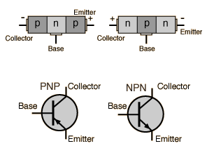
A bipolar junction transistor consists of three regions of doped semiconductors. A small current in the center or base region can be used to control a larger current flowing between the end regions (emitter and collector). The device can be characterized as a current amplifier, having many applications for amplification and switching.
Constraints on operationTransistor operating conditions
Varieties of TransistorsDetails about conduction in transistors
Determining collector currentDetails about base-emitter junction
Index

Semiconductor concepts

Semiconductors for electronics

Electronics concepts
 
HyperPhysics***** Condensed Matter R Nave
Go Back


Transistor as Current Amplifier

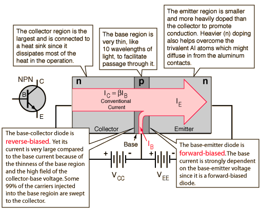
The larger collector current IC is proportional to the base current IB according to the relationship IC =βIB , or more precisely it is proportional to the base-emitter voltage VBE . The smaller base current controls the larger collector current, achieving current amplification.
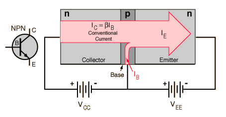
The analogy to a valve is sometimes helpful. The smaller current in the base acts as a "valve", controlling the larger current from collector to emitter. A "signal" in the form of a variation in the base current is reproduced as a larger variation in the collector-to-emitter current, achieving an amplification of that signal.

Constraints on operationComments on structureTo pnp version
Index

Semiconductor concepts

Semiconductors for electronics

Electronics concepts

Reference
Diefenderfer /Holton
p156
 
HyperPhysics***** Condensed Matter R Nave
Go Back


Transistor Structure


The junction transistorCurrent amplifier operation Constraints on operation
Index

Semiconductor concepts

Semiconductors for electronics

Electronics concepts
 
HyperPhysics***** Condensed Matter R Nave
Go Back


Transistor as Current Amplifier

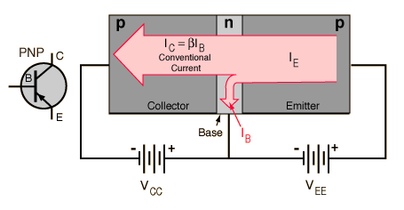
The larger collector current IC is proportional to the base current IB according to the relationship IC =βIB , or more precisely it is proportional to the base-emitter voltage VBE . The smaller base current controls the larger collector current, achieving current amplification.

Constraints on operationTo npn version
Index

Semiconductor concepts

Semiconductors for electronics

Electronics concepts
 
HyperPhysics***** Condensed Matter R Nave
Go Back


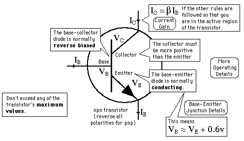
Constraints on Transistor Operation

The bold text and the "buttons" are active links to further details.
Index

Semiconductor concepts

Semiconductors for electronics

Electronics concepts
 
HyperPhysics***** Condensed Matter R Nave
Go Back


Transistor Maximum Values

Part of the manufacturer's data for transistors is a set of maximum values which must not be exceeded in its operation. These form some of the constraints on transistor operation which are a part of the design of any circuit. A typical set, for the silicon transistor 2N2222:

  • Collector-Base Voltage = 60 v
  • Collector-Emitter Voltage = 30 v
  • Base-Emitter Voltage = 5 v
  • Power dissipation = 500 mW
  • Temperature 125 C
Index

Semiconductor concepts

Semiconductors for electronics

Electronics concepts
 
HyperPhysics***** Condensed Matter R Nave
Go Back